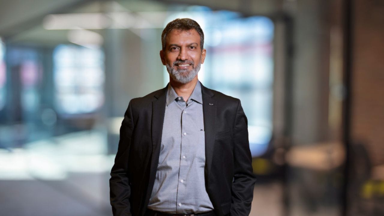






By: Kabilan Jayathungan
India's semiconductor story is often told through the lens of billion-dollar investments, new fabrication facilities, and encouraging government policies. Yet the industry's most critical constraint on top of capital and infrastructure, is talent.
Across the semiconductor value chain, from chip design and validation to manufacturing, packaging, and testing, organizations are competing for a limited pool of highly specialized professionals. The challenge is not simply finding more engineers. It is finding engineers with the depth of expertise required to operate in one of the world's most precision-driven industries.
According to an industry report, India currently has an estimated semiconductor workforce of around 220,000 professionals. Yet by 2027, the industry is expected to face a shortfall of 250,000 to 350,000 skilled workers. In critical domains such as chip design alone, demand could rise by another 275,000 professionals by 2032.
To capitalize on its unique opportunity to become a global semiconductor talent powerhouse, India must shift its focus from merely hiring talent to actively creating it. This transformation requires moving away from isolated initiatives towards fostering ecosystem-wide collaboration, enabling the growth of the necessary skills and expertise across the semiconductor landscape. The semiconductor value chain demands expertise across highly specialized functions, including VLSI design, analog and mixed-signal design, physical design, chip verification and validation, Electronic Design Automation (EDA) tools, Package design, Manufacturing and Process engineering for Fabrication covering Materials, Lithography, etch, deposition, CMP, Yield engineering, statistical process control , device modelling, Process integration & defect learning , Assembly, Test, Marking and Packaging (ATMP).
Why ‘speed’ in talent-building is non-negotiable
Historically, semiconductor talent has been built over long cycles. Design engineers often take years to become industry ready. Fabrication professionals require rigorous hands-on training before they can independently operate in high-stakes manufacturing environments.
But the market no longer has the luxury of time. As global supply chains diversify and nations race to localize chip production, India has a narrowing window to establish itself as a trusted semiconductor hub. At the same time, demand for chips is surging across AI, 5G, automotive electronics, industrial automation, Energy Grids and high-performance computing.
This creates a new reality: organizations must compress time-to-competency by combining industry-grade apprenticeships, modular upskilling, simulated hands-on labs, and employer-led rotations. For example, degree-apprenticeship programs offer classroom theory with supervised shop-floor experience. These shorten the learning curve for fabrication and ATMP roles by exposing trainees to real process variability and yield challenges from day one. Targeting to reduce the time it takes for trainees to become independent operators, reducing the span from years to just a few months.
Additionally, by implementing the design‑focused levers, the organizations, institutes & colleges can accelerate talent development, creating stacked modules for Register Transfer Level (RTL) design, digital verification, analog/mixed‑signal, physical design, device modeling, and EDA tool fluency that map to clear role outcomes. Organizations can also deploy virtual design flows and silicon‑behaviour simulators so that juniors can practice timing closure without tying up scarce silicon and tape‑outs.
AI as the accelerator of semiconductor skills
Artificial intelligence is no longer just a product enabled by semiconductors; it is fast becoming the most powerful tool for building the workforce that designs and manufactures them. On the design side, AI-driven EDA tools are already significantly compressing chip development cycles. But this shift carries a direct implication for talent: engineers who cannot work alongside AI-assisted workflows risk obsolescence before they reach full competency. Training programs that do not reflect this reality are already outdated.
On the learning side, AI-powered platforms can simulate cleanroom environments, replicate EDA tool workflows, and personalize training pathways based on individual progress, effectively compressing time-to-competency in ways traditional skilling never could. If these platforms can reduce the time it takes to bring a fresh engineering graduate to industry-readiness even by 6 to 12 months, the cumulative impact on India's talent pipeline would be significant.
For HR leaders, this demands a dual mandate: build a workforce trained not just on current tools but on AI-assisted design and AI-enabled fab environments and deploy AI actively within skilling infrastructure as an immediate priority.
Building the ecosystem, not just the workforce
No single company can solve this challenge alone. India’s semiconductor talent agenda requires collective action between industry, academia, government, and skilling institutions.
Organizations such as Electronics Sector Skills Council of India are helping establish standardized competency frameworks, while industry bodies continue to drive ecosystem collaboration and industry alignment.
But the next leap will require deeper partnerships, curriculum modernization, apprenticeship-led models, shared lab infrastructure, and stronger industry participation in academic skilling, because semiconductor talent cannot be built in silos.
Call for action
India’s semiconductor story will not be defined solely by the Fabs and ATMP plants it builds, but also by the talent it builds around them. The organizations that succeed will be those that rethink how talent is identified, developed, and continuously reskilled in an environment shaped by rapid technological change and the growing influence of artificial intelligence.
Infrastructure can be funded. Technology can be imported. But skilled talent must be cultivated with intent, with urgency, and at scale.